48V->12V,8V,5V @ 3A BEC (Buck Converter)
- Ishman Mann
- Daniel Puratich
Project whitepaper:
https://warg.365.altium.com/designs/BA1886A1-87A3-459C-B25E-4C3D181A3101
- 1 ToDo:
- 2 Requirements/Needs Assessment
- 3 Architecture
- 4 Component Selection
- 4.1 Buck Converter Components
- 4.1.1 Buck controller
- 4.1.2 Frequency setting resistor
- 4.1.3 Inductor
- 4.1.4 Output Capacitors
- 4.1.5 Input Capacitors
- 4.1.6 Additional Input Capacitor
- 4.1.7 Power MOSFETs
- 4.1.8 Soft-Start Capacitor
- 4.1.9 Feedback Resistors
- 4.1.10 Control Loop Compensation
- 4.1.11 UVLO Resistors
- 4.1.12 ILIM
- 4.1.13 PGOOD Resistor
- 4.1.14 VCC Capacitor
- 4.1.15 BST Capacitor
- 4.1.16 EMI Filter Design
- 4.1.17 SYNCOUT and SYNCIN
- 4.1.18 Anti-ringing snubber
- 4.2 Other Components
- 4.2.1 Input Polyfuse
- 4.2.2 Input TVS
- 4.2.3 Input Common Mode Choke?
- 4.2.4 Input Header
- 4.2.5 Output TVS
- 4.2.6 Output Headers
- 4.2.7 Output LEDs
- 4.2.8 Output Selection “Jumper”
- 4.2.9 Current Sense Amplifier and its Header???
- 4.2.10 Shower Thought on a Vsense line:
- 4.1 Buck Converter Components
- 5 Layout and Manufacturing Considerations
- 5.1.1 Vias
- 5.2 Footprints
- 5.2.1 LM5146RGYR
ToDo:
Add 0 ohm resistors on FET gates
Address review comments
Decide what to do with ground and vias under inductor
Think more deeply about anti-ringing snubber values
Add a bit of an intro/context section to this Confluence
Look into common mode choke (optional)
add in a summary to this confluence page, what this project is, why
Requirements/Needs Assessment
Meets or exceeds spec of Matek BEC 12S-PRO
Externally visible current sense (optional),
needs ADC to interpret op amp value if doing digital comms
Ask FW team for digital (or analog) requirement. (eg. prontocol? CAN? etc…)
Questions:
How many BECs max on the drone?
Depends on the number of peripherals and current requirements
How many peripherals should one BEC connect to (one or multiple)? Would they be same or mixed voltage?
High current devices use one BEC
Some peripherals will share one BEC
Any BEC will only be configured for one voltage, not multiple voltages at once
Which peripherals being applied to, is there a list? Need to see if the spec of Matek BEC is even sufficient for them.
raspberry pi (5.1V input)
servos
video transmitters
radio
lighting
What is the characteristic of the input coming from the PDB to the BEC?
Input range from 9V to 12s (44.4v nominal, 50v fully charged)
Maybe there can be some level of digital control, instead of jumpers? I think this would make it more universal.
Better to have jumpers/switches
(but switches can cause accidents)
Options will definitely include 5(.1)V and 12V, and maybe include 8V.
->Go with 5.1V over 5V since there will be some voltage drop in the harness at higher current. Not doing 5.2V to be safe since some devices have tight 0.1V tolerance on 5V https://ca.robotshop.com/products/benewake-tfmini-s-micro-lidar-module-i2c-12m .
Maybe instead of discrete options, there could be something more continuous involving a potentiometer.
This would be more complex, and is only worthwhile if the target peripherals each have unique input voltage requirements, which is not really the case
Linear or Switching BEC?
Definitely switching since more efficient and less heat (although more noisy).
Could optocoupler serve any purpose?
Not sure, will research more
Should current sense be accessible as an analog or digital value?
Digital will probably end up using some CAN protocol, in which case the ADC output needs to be passed through a microcontroller and then to the CAN driver and connector.
Analog will be less reliable and need some digital conversion on the part of other components on the drone.
Should external current sense go before or after the buck converter (or both)?
1) Output side in series with load
Pros
Get to see what the peripheral is drawing from the BEC.
Cons:
Sense resistor on output side may introduce a small voltage drop that varies depending on the current. This may decrease and maybe somewhat destabilize output voltage (adds error).
However, I think a 2 mOhm max current sense resistor w/ amplifier will hardly have any voltage drop.
1.1) Another option: output side in series with the Buck converter inductor
Pros
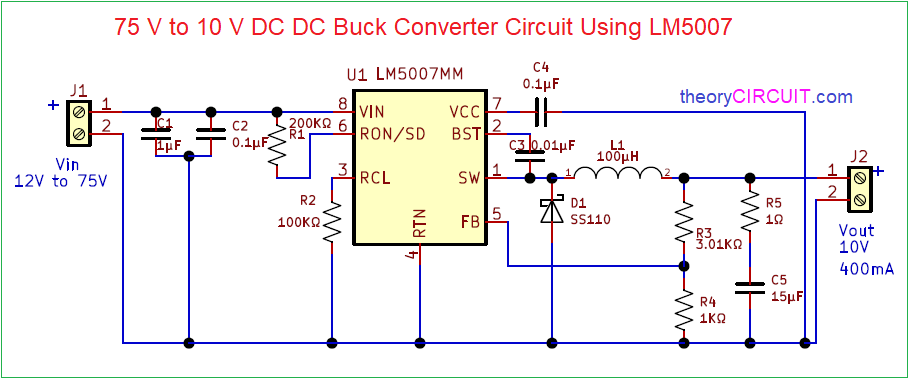
If I have something like in this image https://theorycircuit.com/wp-content/uploads/2021/02/75-V-to-10-V-DC-DC-Buck-Converter-Circuit.png, but an extra sense resistor is in series with the inductor, wont the feedback mechanism just account for the error created by the sense resistor?
Cons:
This just gives the current passing through the MOSFET (& other elements) within the buck converter IC, not particularly the output or input. The usefulness of this sensing this is questionable.
Also, the inductor current will have a much wider ripple range than the load current.
2) Input side in series with supply:
Pros:
Get to see what the BEC as a whole is drawing from the battery. This might be more valuable in the context of the system.
Also, if the efficiency of the BEC is tested and proven to be in some range (e.g. 85-95%), then peripheral current draw can be estimated from BEC current draw.
Cons:
Higher current on input side, so more power consumed by current sense resistor.
Then again, the highest current drawing is probably the 3A of the RPI. Even if the input current is something extreme like 20A, (20A^2)*2mOhms = 0.8W, which compared to what the peripheral itself would be drawing, is negligible.
Current sense would be on a signal that is switching on and off. One would have to obtain an average current using a microcontroller, which introduces some complexity.
3) Both sides:
Pros:
Accurate BEC efficiency tracking. But this is not really necessary
Cons
All the cons from the input side + output side.
Deciding how to create multiple voltage output options
1) one adjustable buck using jumpers
Cheapest option, but has the technical challenge of figuring out the jumper/resistor configuration.
Makes the most sense since each BEC will only power devices of the same voltage.
1.1) one adjustable buck using a potentiometer
Cheap, involves less jumpers, and offers more flexibility in output voltage
But, it’s technically complex. Also, is the flexibility even needed?
2) multiple bucks
Expensive, but effective and technically simpler.
3) one buck with multiple LDOs connected to it
Medium price and simple/effective, but high power consumption.
Overcurrent protection and thermal shutdown
Simplest option is to just pick a buck IC that has these features built in, just as the Matek BEC does with the LM5116
Spike protection?
Depends on the characteristics of the input LIPO battery, PDB, and loads…
e.g. TVS diode (unidirectional), flyback diode, snubber circuit…
External current limiting on output
1) dedicated circuitry, e.g. https://www.youtube.com/watch?v=8uoo5pAeWZI&ab_channel=GreatScott!
This would be cool but quite a technical challenge to implement.
2) simple fuse
3) Nothing external
It may be simplest to pick a buck with preexisting current limiting feature, which a lot of them have. In this sense, it may be best to wait on whether to have external output current limiting until the part selection stage
What happens if you short circuit the output of a boost converter?
https://www.renesas.com/us/en/document/whp/how-protect-buck-regulators-overcurrent-damage
Load flyback diode (separate to the one used in the buck converter)
For inductive loads like servo
https://www.youtube.com/watch?v=LXGtE3X2k7Y&ab_channel=Afrotechmods
Does control circuit inside our servos deal with the back EMF? It should, but an extra layer of safety on BEC is needed
It may be the case that the diode used for the buck converter is enough of a flyback for inductive load, so a 2nd diode is not needed. To be determined during part selection.
Actually, considering some analysis the load side diode would act as a clamp, not a flyback. That means choose a TVS or Zener diode (TVS has faster response to transients). Nonetheless it will help with voltage spikes.
Snubber on Buck converter and other output side diodes
The need for this depends on the buck converter IC chosen during part selection.
Polyfuse vs normal fuse
Polyfuse is resettable and there are ones that don’t instantly trigger on overcurrent, so switching current transients won’t trigger them.
Other bonus features?
Need to consider how output to USB C for rpi will work
Consider adding useful common output terminals as an a feature.
Or, have a simple generic output terminal to minimize board weight and size. The simple terminal can be connected to the needed adapter cable.
Something useful should be done with the current sense
Option A) Current sense terminal will be useful if there is also a terminal to the enable pin of the buck converter for another board to turn it off
Option B) If a buck controller/converter with adjustable current limiting is present, current sense resistor will be useful to limiting current of the buck/
In this case, there may not be a need to provide terminals for another board to read the current sense and control the enable, it would just be a bonus item at that point
Architecture
Some notes:
Input will be 2S (around 6V lowest) min not 5V.
Using 3 output LEDs is wasteful. 0 is enough.
There might need to be different TVS diodes for the different output voltages. → Nah
Sense Option A)

Sense Option B)

Buck IC options
Caters Sense Option A
(full on converter chips)
1) https://www.ti.com/product/TPS54560B
4.5-60V Vin
0.8-58.8 Vout
5A Iout max
Frequency synchronization, Light Load Efficiency, Over Current Protection,
2) https://www.digikey.ca/en/products/detail/analog-devices-inc/LT1170HVCT-PBF/891558
3-60V Vin
1.244-75V Vout
5A Iout max
Fancy features
$31.20
3) https://www.monolithicpower.com/en/mp4575.html
4.5-55V Vin
1-49.5V Vout
5A Iout max
Caters Sense Option B:
(just controller chips, needs external FETs. More design flexibility):
4)https://www.ti.com/product/LM5148
$6.63 DigiKey
5) https://www.ti.com/product/LM5149
$6.75 DigiKey
6)https://www.ti.com/product/LM5088
$5.82 DigiKey
7)https://www.ti.com/product/LM5085
$4.49 DigiKey
8)https://www.monolithicpower.com/en/mp2908a.html
$4.29 DigiKey
9) https://www.monolithicpower.com/en/mp9928.html
$4.14 DigiKey
10) https://www.ti.com/product/LM5146?keyMatch=LM5146&tisearch=search-everything&usecase=GPN-ALT
Component Selection
Buck Converter Components
Latest TI Design Calculation Tool plug and chug excel file (ignore the file name):
^This is the tool I used to verify/finalize all values
Buck controller
LM5146:

Frequency setting resistor
RRT = 45.3kR, 1/16W
Yields ~220KHz switching frequency. Lower frequency means less switching loss. Can’t go too low or too large inductor and output capacitors will be needed to account for the higher ripple.

Inductor

LF = 27uH, (saturation at > 5.375A, > 4.3A max DC current. See ILIM section)
Alternative: https://www.digikey.ca/en/products/detail/sumida-america-inc/125CDMCCDS-470MC/9490421
Has a pretty bad DCR of 97.2mOhm. Need to find/consider an inductor with <= 40mOhm DCR to save about 3% efficiency at nominal I/O conditions.
https://www.desmos.com/calculator/cmd60zlxtp
At 220KHz, 3A peak load, 27uH gets ripple between 25%-50% over the entire output range.


Output Capacitors


COUT = 3 x 22uF, 25V, ceramic, X7R, 1206 or 1210 size
https://www.digikey.ca/en/products/detail/murata-electronics/GRM21BR61E226ME44K/4905534
ESR of each capacitor = 3mR at 220KHz according to SimSurfing. For 3 in parallel ZTotal = (Z1^-1 + Z3^-1 + Z3^-1)^-1 = 0.001 - j0.10961. That is, 3mR becomes 1mR for 3 capacitors.
https://www.desmos.com/calculator/iwoiula6yw
Lower capacitance value (30.838uF) is needed to achieve an optimal s <= 1% ripple. But, for 12s nominal input to 5.1V output, TI design calculation tool recommends de-rating to 47uF. Using 3 x 22uF for low ESR.
Here input voltage is X axis and capacitance is Y axis:
Ceramic cap.s have low ESR. Higer ESR increases capacitance needed.


Input Capacitors


CIN = 6 x 4.7uF, 100V, ceramic, X7R, >2.52 RMS current
Option: GRJ31CZ72A475KE01L
10mR ESR per capacitor. Approximate ESR for 6 in parallel is 10mR/6 = 1.67mR
https://www.desmos.com/calculator/uovqhzl57b
To achieve an optimal 2% ripple:
At 5.1V out, 21.98uF minimum capacitance is needed (at 7.5V in).
At 8V out, 13.471uF minimum capacitance is needed (at 11.8V in).
At 12V out, 8.772uF minimum capacitance is needed (at 17.5V in).
TI design calculation tool recommends de-rating to 6 x 4.7uF
https://www.desmos.com/calculator/x1iysyhtb4
2.52 RMS rating computed from a de-rated 5A output (1.8 RMS rating if de-rating to 3.5A)
Here D = 0.5 gives the maximum value:
Per the TI design tool recommendation:
Max ESR for 2% ripple at 5V is 15mR
Max ESR for 2% ripple at 8V is 25mR
Max ESR for 2% ripple at 12V is 39mR (7mR for 1%, which parallel capacitors can achieve)


Additional Input Capacitor
From LM5146 datasheet Section 10:
I think the CD chosen in the EMI Filter section should be enough to deal with this.

Power MOSFETs

https://www.desmos.com/calculator/o9jukbktfa
Power loss calculations assume nominal conditions: 3A, 45V in, 5V out. (Note: Nominal is updated to 5.1V output, but the power analysis results in the below table/graphs should be effectively the same.)
Assuming 14ns tdt1 and tdt2, which is the LM5146 default.
Option | |||||
|---|---|---|---|---|---|
Cost | $2.52 | $1.47 | $2.05 | $2.51 | $2.62 |
VDSS | 80V | 60V | 60V | 60V | 60V |
Max IDS | 74A | 69A | 100A | 100A | 100A |
Max temp | 150C | 150C | 150C | 150C | 150C |
Rth | 50C/W | 50C/W | 50C/W | 50C/W | 50C/W |
RDS | 6.2mR | 7.8mR | 5.7mR | 3.3mR | 2.8mR |
tR | 7ns | 5.5ns | 6.3ns | 12ns | 5ns |
tF | 5ns | 2ns | 1.7ns | 7ns | 5ns |
QG | 24nC | 17nC | 15nC | 27nC | 33nC |
QRR | 37nC | 54nC | 63nC | 28nC | 65nC |
VF | 0.9V | 0.8V | 0.8V | 0.9V | 0.9V |
Pcond1 calculated | 0.0063041W | 0.0079310W | 0.0057957W | 0.0033554W | 0.0028470W |
Pcond2 calculated | 0.050433W | 0.063448W | 0.046366W | 0.026843W | 0.022776W |
Psw calculated | 0.17153W | 0.099708W | 0.10347W | 0.26548W | 0.1485W |
Pgate calculated | 0.0396W | 0.02805W | 0.02475W | 0.04455W | 0.05445W |
PRR calculated | 0.3663W | 0.5346W | 0.6237W | 0.2772W | 0.6435W |
PcondBD calculated | 0.016632W | 0.014784W | 0.014784W | 0.016632W | 0.016632W |
PQ1 = Pcond1 + Psw + Pgate | 0.21744W | 0.13569W | 0.13401W | 0.31339W | 0.20580W |
TQ1 = PQ1*Rth + Tambient=25C | 35.872C | 31.78C | 31.701C | 40.669C | 35.290C |
PQ2 = Pcond2 + Pgate + PcondBD + PRR | 0.47297W | 0.64088W | 0.70960W | 0.36523W | 0.73736W |
TQ2 = PQ2*Rth + Tambient=25C | 48.648C | 57.044C | 60.480C | 43.261C | 61.868C |
Comments | Good for Q2 | Good for Q2 | Good for Q1 | Good for Q2 | Good for Q1 |
Some example combos:
1) CSD18563Q5A and CSD18534Q5A

2) BSC034N06NSATMA1 and BSC039N06NSATMA1

3) CSD18563Q5A and BSC039N06NSATMA1

Although Combo 3 has appx. 1% better efficiency, Combo 1 has some benefits. Both MOSFETS would be of the same brand and have similar rise/fall time. Also, Combo 1 is $1.04 cheaper overall.
Q1 = CSD18563Q5A
Q2 = CSD18534Q5A
Soft-Start Capacitor

Css = 16V, 680nF X7R
Yields 54.4ms startup time. Longer time will help lower inrush currents.
It seems 54.4ms is more than good enough, even overkill, to ensure that ICAP is small


Feedback Resistors
RFB1 = 21kR, 1/16W
3 different RFB2 will be jumper selected for the different output voltage options, such that input on FB pin of LM5146 is 0.8V.
For 5.1V: RFB2_5V1 = 3.92kR, 1/16W
Note: There may be a case that 5.2V output is realized to be more appropriate due to power harness resistance loss. In this case, use 3.83kR instead.
For 8V: RFB2_8V = 2.32kR, 1/16W
For 12V: RFB2_12V = 1.5kR, 1/10W
Control Loop Compensation

Desired crossover frequency is typically chosen to be 10% to 20% of of the switching frequency, so 33kHz is a good pick.
Zeros and poles are placed per TI design tool recommendation.
2 compensator zeros are placed just before the LC double pole.
The 1st compensator pole is placed near the zero created by COUT and it’s ESR. Since the ESR of the COUT currently chosen is so low (1mR but assuming 2mR worst case) the first pole is at a very high frequency (not even visible on the Bode Plot).
The 2nd compensator pole is half the switching frequency.
Phase shift is between 50% to 70% at crossover frequency, for all 3 output voltages, which is what is recommended.


Thus,
RC1 =12.1kR, 1/16W
CC1 = 4700pF, 50V
CC2 = 120pF, 50V